What are CVD Diamonds?

Chemical vapor deposition is a method by which diamond can be grown from a hydrocarbon gas mixture. Since the early 1980s, this method has been the subject of intensive worldwide research. Whereas the mass-production of high-quality diamond crystals make the HPHT process the more suitable choice for industrial applications, the flexibility and simplicity of CVD setups explain the popularity of CVD growth in laboratory research. The advantages of CVD diamond growth include the ability to grow diamond over large areas and on various substrates, and the fine control over the chemical impurities and thus properties of the diamond produced. Unlike HPHT, CVD process does not require high pressures, as the growth typically occurs at pressures under 27 kPa.


Hardness

Synthetic diamond is the hardest known material, where hardness is defined as resistance to indentation. The hardness of synthetic diamond depends on its purity, crystalline perfection and orientation: hardness is higher for flawless, pure crystals oriented to the direction (along the longest diagonal of the cubic diamond lattice).Nanocrystalline diamond produced through CVD diamond growth can have a hardness ranging from 30% to 75% of that of single crystal diamond, and the hardness can be controlled for specific applications. Some synthetic single-crystal diamonds and HPHT nanocrystalline diamonds (see hyperdiamond) are harder than any known natural diamond.
Impurities and inclusions

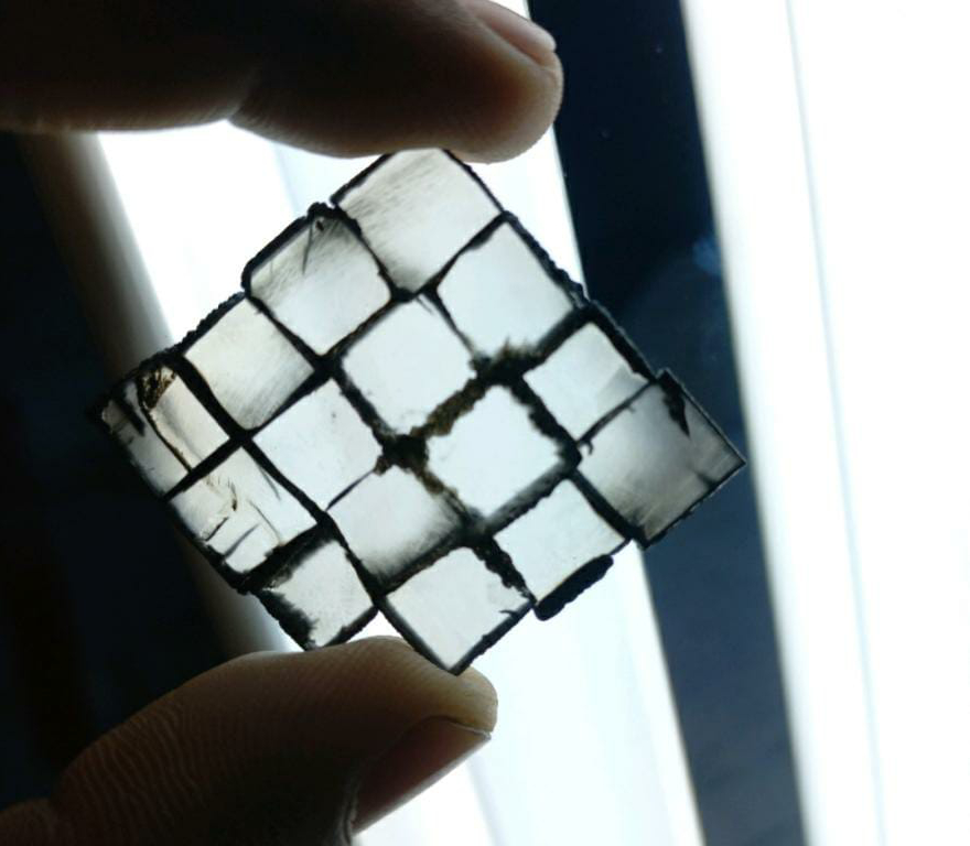
Every diamond contains atoms other than carbon in concentrations detectable by analytical techniques. Those atoms can aggregate into macroscopic phases called inclusions. Impurities are generally avoided, but can be introduced intentionally as a way to control certain properties of the diamond. Growth processes of synthetic diamond, using solvent-catalysts, generally lead to formation of a number of impurity-related complex centers, involving transition metal atoms (such as nickel, cobalt or iron), which affect the electronic properties of the material.
For instance, pure diamond is an electrical insulator, but diamond with boron added is an electrical conductor (and, in some cases, a superconductor), allowing it to be used in electronic applications. Nitrogen impurities hinder movement of lattice dislocations (defects within the crystal structure) and put the lattice under compressive stress, thereby increasing hardness and toughness.


Thermal conductivity

The thermal conductivity of CVD diamond ranges from tens of W/m-K to more than 2000 W/m-K, depending on the defects, grain boundary structures. As the growth of diamond in CVD, the grains grow with the film thickness, leading to a gradient thermal conductivity along the film thickness direction.
Unlike most electrical insulators, pure diamond is an excellent conductor of heat because of the strong covalent bonding within the crystal. The thermal conductivity of pure diamond is the highest of any known solid. Single crystals of synthetic diamond enriched in 12
(99.9%), isotopically pure diamond, have the highest thermal conductivity of any material, 30 W/cm·K at room temperature, 7.5 times higher than that of copper. Natural diamond’s conductivity is reduced by 1.1% by the 13
naturally present, which acts as an inhomogeneity in the lattice.
Diamond’s thermal conductivity is made use of by jewelers and gemologists who may employ an electronic thermal probe to separate diamonds from their imitations. These probes consist of a pair of battery-powered thermistors mounted in a fine copper tip. One thermistor functions as a heating device while the other measures the temperature of the copper tip: if the stone being tested is a diamond, it will conduct the tip’s thermal energy rapidly enough to produce a measurable temperature drop. This test takes about 2–3 seconds.
